
KLA Instruments Innovation History
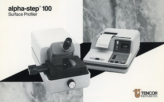
The Alpha-Step® 100 is the first product of Tencor Instruments.
The Alpha-Step provides impressive improvements in step height measurement accuracy and repeatability over the existing competitive products. With its attractive pricing, small form factor, and improved functionality, it is soon considered a critical quality control tool in most semiconductor fabrication plants, or fabs.
Learn more about our latest offerings in this product series:

Nano Instruments, Inc. releases the first commercially available nanoindenter, called the Nano I.
The first commercially available nanoindenter, the Nano I system, is released by Nano Instruments, a company formed by the inventors of nanoscale mechanical testing technology, Dr. Warren Oliver and Sir John Pethica. The core technology of the force-displacement nanoindenter includes electromagnetic actuation, chosen for its unmatched stability, combined with a 3-parallel plate capacitor to measure displacement. This superior technology has withstood the test of time and is used today in KLA nanoindentation systems.
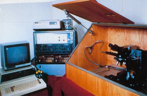
The Alpha-Step 200 tool releases with 2x faster scanning than the competition, a CRT monitor to display the scan profile, plus computer-controlled automated measurement, leveling and calculations.
The new Alpha-Step 250 features an enhanced sensitivity down to 1Å, using an acoustic enclosure to isolate the measurement from the environment.
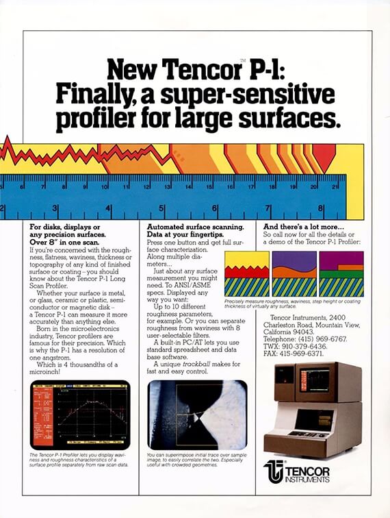
The Tencor P-1 Long Scan stylus profiler is the first in the industry to offer ultra-flat 200mm scans in a single profile, without the need to stitch.
The release of the P-1 Long Scan profiler features a revolutionary new design, with industry-first innovations to the scanning stage, optics, and sensor technology-—innovations that provide rock-solid stability, unbeatable sensitivity and repeatability. The system features an ultra-flat scanning stage capable of high-resolution scans up to 200mm in a single scan, enabling characterization of surface roughness, waviness, and thin-film stress. The new stage is also the industry’s first 3D scanning stage, adding a third dimension to characterize surface topography. The system features the first top-view optics to provide a clear view of the sample, free of distortion from the traditional angled side-view. Finally, the sensor technology incorporates the industry’s first and only linear variable differential capacitor (LVDC), resulting in sub-Angstrom electronic resolution with a low moment of inertia, enabling low force control and reducing sensitivity to noise.
Learn more about our latest offerings in this product series:
Dr. Warren Oliver and Sir John Pethica are awarded a patent for the Continuous Stiffness Measurement (CSM) technique, representing the biggest innovation in nanomechanical testing.
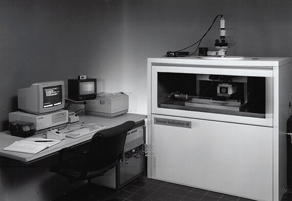
The Nano Indenter® II is released with a new Continuous Stiffness Measurement (CSM) technique for dynamic nanoindentation. Dr. Warren Oliver and Sir John Pethica are awarded a patent for the CSM technique, which enables continuous measurement of hardness and modulus as a function of depth. This measurement technique also allows the user to extract dynamic mechanical analysis (DMA) data from indentation tests. The CSM technique remains the single biggest innovation in the nanoindentation field since the development of the first nanoindenter.
Nano Instruments introduces a High Load actuator capable of indentation loads up to 5000mN.
The Tencor P-2H is the industry’s first profiler to support an automated wafer and disk handler to minimize defects introduced by the operator touching the samples.
The Tencor P-2 open frame offers users the flexibility to load samples up to 430mm by 430mm while the Tencor FP-2 provides support for the flat panel industry by enabling scans of samples up to 630mm by 630mm.
Dr. Warren Oliver and Dr. George Pharr publish an article that will be cited more than 30,000 times.
Dr. Warren Oliver and Dr. George Pharr publish “An improved technique for determining hardness and elastic modulus using load and displacement sensing indentation experiments” in the Journal of Materials Research. This paper lays the foundation for measuring nanoscale mechanical properties of hardness and elastic modulus. This seminal work enables semiconductor manufacturers to prevent failure in thin films by quantitatively linking processing parameters with the mechanical strength and flexibility of the film. The same year, Nano Instruments introduces a lateral force measurement option, enabling surface profiling and 3D topographic mapping of indentations.

Click here to read the original paper
An improved technique for determining hardness and elastic modulus using load and displacement sensing indentation experiments.
Enhanced optics bring Nomarski Interference Contrast and brightfield/darkfield imaging to the Olympus microscope used on the Nano Indenter II to help users find measurement features on low contrast samples.
Nano Instruments, Inc. launches the affordable Nano Indenter IIs system for the razor-blade industry by redesigning the actuator and simplifying the optics.
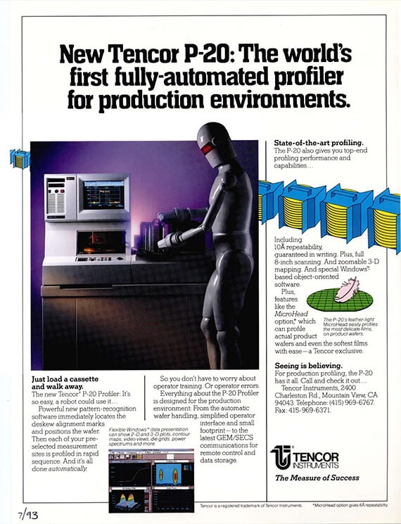
The Tencor P-20 is the industry’s first fully automated stylus profiler, from placing the wafer cassette on the tool to final measurement results. To accomplish full automation, the P-20 adds pattern recognition and SECS/GEM in combination with the existing handler.
The Alpha-Step 500 builds on the success of the previous products by adding the capability to measure features up to 1mm in height, plus new high magnification optics and a color camera.
Nano Instruments opens new headquarters in Oak Ridge, Tennessee.
Filmetrics® F20 – The world’s first compact, easy-to-use thin-film measurement instrument.
The F20 is the first of its kind: an instrument using a miniature fiberoptic spectrometer to measure thin-film thickness. White light reflecting from a surface coated with a thin film is analyzed to measure the film thickness, utilizing the characteristic signature created by coherent interference. Leveraging the rapidly growing computational power of desktop personal computers and modern graphical user interface software, the F20 is easy to use, compact, and offered at a price point that makes it accessible for users in applications that previously could not afford to accurately measure their films.
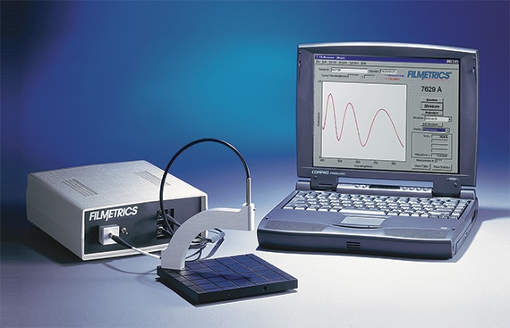
Learn more about our latest offerings in this product series: Filmetrics® F20
The Nano Indenter XP launches with the new XP Head actuator, which continues to be in production to this day. This new actuator technology streamlines measurement setup, and improved load-frame stiffness reduces systematic error while expanding the range of indentation.
The release of the Tencor P-10, P-11, P-12, and P-22 feature the latest innovations in low force control, the capability for steps up to 1000µm, and enhanced environmental isolation.
The Microhead II enhances the linear variable differential capacitor (LVDC) with the addition of recipe-controlled low force, down to 0.05mg. It adds constant force control by dynamically adjusting the force on the pivot so that the same force is applied on the sample surface regardless of the step height. In addition, a new sensor is available to support step heights up to 1000µm. The P-12 adds new acoustic isolation skins and an active isolation table, enhancing isolation from environmental noise, enabling measurement of the roughness of super-smooth hard drive discs. The P-22 adds an isolation table to the existing P-20 handler-based system for fully automated measurements that include wafer handling capability, pattern recognition, and SECS/GEM, improving production efficiency with a total solution for semiconductor industry.
Learn more about our latest offerings in this product series:
We introduce the Filmetrics F30, a reflectance-based deposition-rate monitoring instrument built to monitor the growth of epitaxial semiconductor crystals.
The Dynamic Contact Module (DCM) enables ultra-low-load indentation to enable testing of polymers and other viscoelastic materials. Ultra-low-load nanoindentation is made possible by the low mass and high resonant frequency of the DCM actuator.
The Tencor P-30 replaces the open cassette handler with a SMIF handler and a mini-environment inside the system to support new low particle requirements of the semiconductor industry.
Tencor Instruments and KLA Instruments merge to become KLA-Tencor, Inc., the world leader in yield management and process control solutions for semiconductor manufacturing and related industries.
The HRP®-220 is a breakthrough for inline surface metrology with an industry-first patented dual-stage stylus profiler, combining the long scan stage of the P-22 with a high-resolution piezo stage and the DuraSharp® stylus to enable fine-feature measurement and analysis.
Filmetrics F30 wins R&D 100 award.
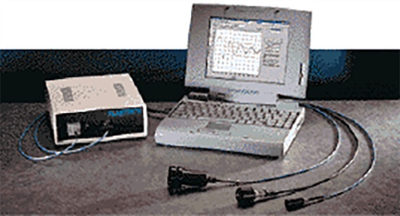
The Filmetrics F30 performs in situ, real-time deposition-rate monitoring during MOCVD or MBE growth of epitaxial semiconductor layers. Using the virtual interface technique developed at Sandia National Labs1, the F30 continuously measures light reflected from the sample surface to monitor crystal growth rate. Because the Virtual Interface technique is independent of the underlying layer structure, alloys of different compositions can be deposited in sequence on a single wafer to rapidly calibrate growth rate and composition of several different materials.
1Breiland, W. & Killeen, Kevin. (1996). A virtual interface method for extracting growth rates and high temperature optical constants from thin semiconductor films using in situ normal incidence reflectance. Journal of Applied Physics. 78. 6726 – 6736. 10.1063/1.360496.
Learn more about our latest offerings in this product series: Filmetrics F30
Filmetrics adds the capability to measure refractive index (n) and extinction coefficient (k) on the F20 and F30.
Filmetrics F20 and F30 systems can now measure thickness and optical constants for each film in a multi-layer stack.
Filmetrics F20 and F30 systems now use a standard parallel-port interface, eliminating the need for an analog interface card and facilitating use with a customer-supplied PC.
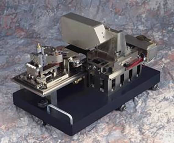
The first Candela® Instrument optical surface analyzer (OSA) is introduced to characterize surface defects for the hard disk drive (HDD) industry.
The Candela optical surface analyzer (OSA) is a multi-channel laser-based defect inspection system for R&D and process monitoring, designed specifically for the HDD industry. The new inspection system characterizes surface defects such as particles and scratches on disk substrates and finished media, providing significant advantages over traditional manual visual inspection.
Learn more about our latest offerings in this product series: Hard Disk Inspection Systems
MTS Systems Corp. acquires Nano Instruments, Inc.
The HRP-320 extends the capability of the HRP-220 to 300mm wafers, with the industry’s first and only system capable of measuring the full diameter of a 300mm wafer in a single scan. This tool also offers a dual stage and the first fully automated measurements using a 200mm/300mm handler system.
Photonics Spectra gives the Filmetrics F20 the Circle of Excellence award, recognizing it as one of the world’s top 25 technically innovative photonics products.
The Filmetrics F40 small-spot measurement instrument attaches to a standard microscope to enable film thickness measurement with a spot size as small as 10µm.
The Filmetrics F20 and F30 can now be configured with a UV spectrometer, covering wavelengths from 215nm to 670nm and reducing the minimum film thickness that can be accurately measured from 10nm to 3nm.
The R-Theta stage on the Filmetrics F50 motorized mapping instrument accepts up to 200mm diameter wafers, allowing the system to measure and display the film thickness at user-defined locations.
By continuously monitoring the reflected light spectrum during chemical mechanical planarization (CMP) the Filmetrics F76 in situ CMP endpoint detection system enables precise determination of process endpoint.
MTS releases a high temperature option: a 100°C test chamber designed to enclose the entire Nano Indenter XP system.
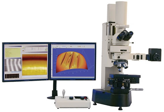
ADE Phase Shift releases the MicroXAM optical profiler, with Angstrom-level sensitivity in phase shifting interferometry for super smooth surfaces and vertical scanning interferometry for samples with larger step heights.
Learn more about our latest offerings in this product series:
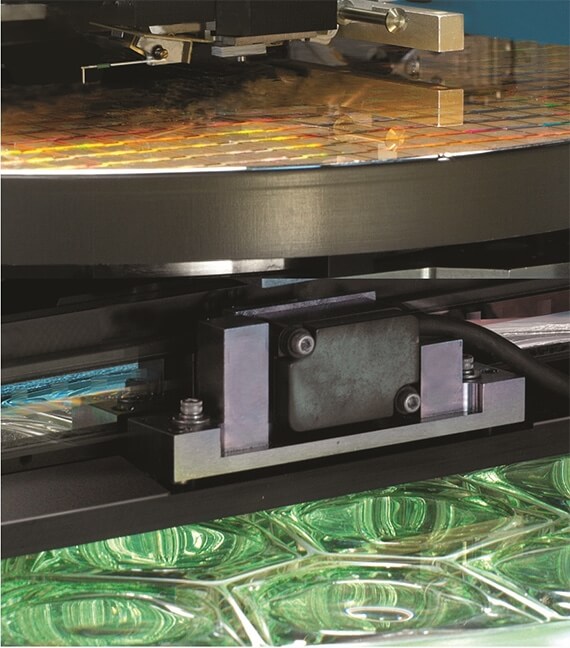
The HRP-240 and HRP-340 represent significant enhancements to the HRP product lines by improving the ease of use, throughput, and precision.
A new piezo flexure stage design is added to minimize out-of-plane motion, improving scan flatness by >2x over the previous design, while maintaining the 90µm by 90µm scan area with 1nm resolution. The system adds inline high and low magnification optics and utilizes the proximity sensor to enable no-touch autofocus, allowing fast, precise focus plus improving stylus lifetime by reducing the number of stylus touches on the surface. The long-scan stage is improved by the addition of linear encoders for more accurate sample positioning, plus higher resolution with a finer pitch leadscrew. Overall system performance is improved by the addition of a digital signal processor to handle all stage controls, reserving the computer processing power for the user interface. Finally, Dipping Mode™ enables measurement of high aspect ratio etch depth features.
Learn more about our latest offerings in this product series:
The TS 2100 extends hard disk drive (HDD) tribology capability by adding magnetic imaging and measurement of the carbon layer and lubricant layer. The TS 2100 also includes improvements to measurement sensitivity, speed and resolution.
The release of TestWorks software for the Nano Indenter XP brings a modern Windows-based operating system to nanoindenter operation and data analysis.
The OSA 5100 and 5120 are the fifth generation Candela OSA systems, adding disk surface topography measurement. The OSA 5120 is equipped with an automated disk cassette-to-cassette handler to deliver defect detection and classification capability to high volume HDD manufacturing.
MTS introduces several new products, including a 300mm wafer test system, the Nano Indenter XPW; a compact benchtop system, the Nano Indenter SA2; and an integrated imaging system, the Nano Tribology Workstation.
The Tencor P-15 combines the P-10 and P-11 systems to offer a complete surface topography measurement system to support both R&D and production environments on a single platform.
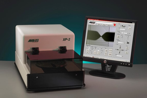
Ambios Technology releases the XP1 and XP2 stylus profilers that feature the industry’s first and only systems with patented optical lever sensor technology.
The XP1 and XP2 stylus profilers from Ambios Technology introduce an optical lever sensor technology adapted from the Atomic Force Microscope (AFM). The optical lever sensor enables faster scanning while maintaining accurate surface profiling. The novel sensor combined with low force control and support for samples up to 200mm provides customers an affordable surface topography measurement solution.
Learn more about our latest offerings in this product series:
Using a hyperspectral imaging system, the Filmetrics STMapper whole-wafer imaging instrument maps film thickness data across wafers as large as 200mm diameter with a 50µm spot size in less than 5 seconds.
R&D magazine gives the Filmetrics STMapper an R&D 100 award, recognizing it as one of the 100 most significant new products of the year.
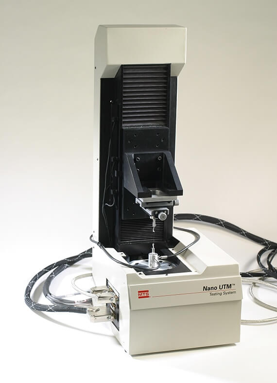
The NanoUTM is released to measure tensile properties of fibers, finding a unique application in measuring spider silk.
The NanoUTM and NanoBionix instruments are released, designed for measuring the tensile properties of fine single fibers. This application is rapidly adopted by the spider-silk industries because of its ability to link the genome of many spider species to the mechanical properties of their silk. The NanoUTM generates interest from advanced textile research and development engineers because it can quantify viscoelastic properties of polymer microfibers at constant strain rates up to 400%.
Learn more about our latest offerings in this product series:
1000th Filmetrics thin film measurement instrument is shipped.
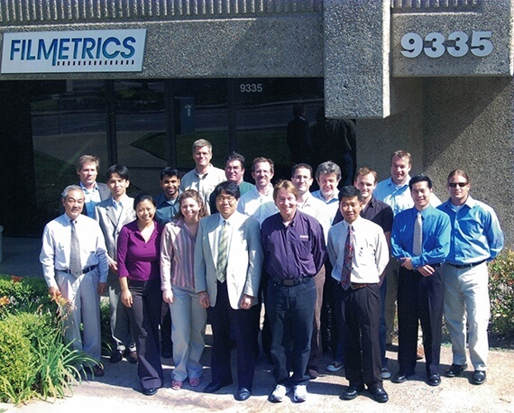
Filmetrics now sells more thin-film measurement instruments than any other manufacturer. This high adoption is due to the rapid, high-quality support of the Filmetrics application team combined with the ease-of-use and affordability of the instrument. The instrument software, FILMeasure® for instruments with a manual stage and FILMapper™ for motorized stages, has been continuously enhanced, adding a significant number of new features and improved performance.
Learn more about Filmetrics: Filmetrics
The new Candela CS1 and CS2 systems address compound semiconductor wafer inspection applications, providing the unique capability to inspect both transparent and opaque wafers for detection and classification of particles and other process-related defects.
The Nano Indenter XP platform is enhanced with a 200°C hot stage and improved optics.
The Alpha-Step IQ takes the proven performance of the Alpha-Step 500 and adds new USB electronics and completely redesigned software to significantly improve the ease-of-use and provide enhanced scan sequencing and data analysis capability.
The parallel port interface is replaced with a USB interface in all Filmetrics instruments, facilitating use with newer computers.
An improved Vis-NIR spectrometer becomes the standard-configuration spectrometer on all Filmetrics thin-film measurement instruments, covering a wavelength range of 400nm to 1000nm and enabling measurement of films from 15nm to 50µm thick.
All instruments can now be configured with an NIR spectrometer that covers a wavelength range of 950 to 1700nm and can measure films from 100nm to 100µm thick.
Filmetrics introduces the F20-EXR, which includes both a visible and NIR spectrometer, enabling Filmetrics instruments to measure films from 15nm to 100µm thick.
The Candela OSA 6100 and 6120 series systems introduce X-Beam channel technology, adding radial illumination to the existing circumferential illumination design, plus advanced collection optics that extend defect sensitivity down to 80nm. This multi-channel system simultaneously detects and classifies defects such as particles, pits and stains; characterizes lubricant thickness, and uses the Kerr Effect to characterize magnetic imaging.
The NanoVision feature is added to the product portfolio, enabling basic scanning probe microscopy using the indenter tip and a high-resolution piezo nanopositioning stage.
KLA-Tencor acquires Candela Instruments, the leading supplier for laser-based surface inspection systems optimized for the data storage industry, measuring metal and glass substrates, plus finished media.
Filmetrics introduces the F80 – a high speed patterned wafer film thickness measurement system.
The Filmetrics F80 is a high-speed, small-spot, hyperspectral-imaging film thickness measurement instrument. It performs measurements on patterned wafers up to 200mm in diameter. The hyperspectral imaging system utilizes a revolutionary pattern recognition technique that can distinguish regions in the field of view based on their film stack, composition, and thickness.
Learn more about our latest offerings in this product series: Filmetrics F60
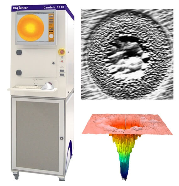
The Candela CS10 and CS20 system are released for inspection of defects on power devices, high brightness LEDs, and other compound semiconductor devices.
The new Candela CS10 and CS20 systems are designed to replace manual visual inspection of compound semiconductor wafers with automated defect inspection. These second-generation Candela CS systems also introduce a new defect location trace-back feature to facilitate offline defect review. The CS10 and CS20 systems provide advanced surface analysis for detection and classification of a variety of defects for power devices, high brightness LEDs, specialty coatings on glass, CMOS image sensors and LCoS displays.
Learn more about our latest offerings in this product series:
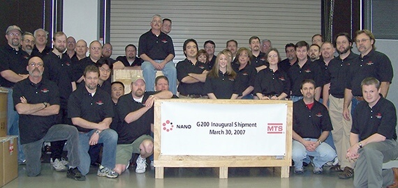
The Nano Indenter G200 is the first ISO 14577 compliant nanomechanical tester.
The Nano Indenter G200 is the first commercially available nanoindenter designed to comply with the ISO 14577 standard, the international standard for instrumented indentation testing. The system can measure high loads up to 10N, bridging the gap between nanoindentation and Vickers hardness testing. Lateral force measurement capability enables scratch and wear testing. Large samples can be measured with a 200mm by 200mm sample stage. The NIDAQ Expansion system allows users to read and control external devices, enabling the addition of third-party cameras and other sensors, such as temperature and humidity.
Learn more about our latest offerings in this product series:
KLA acquires ADE Corporation, adding the MicroXAM-100 optical profiler to KLA’s benchtop metrology portfolio, along with substrate geometry and defect inspection solutions for the semiconductor market.
Using a hyperspectral imaging system, the Filmetrics F42 micro-spot mapping instrument produces a thickness map image with a pixel size as small as 3µm.
The Candela 6300 and 6320 series systems include design improvements that deliver the wide spatial bandwidth and low noise floor required for accurate measurement of surface roughness and waviness measurements of HDD substrates.
The Tencor P-16+ offers improvements to the industry-leading P-15: new USB electronics, enhanced software, plus Apex advanced data analysis and report writing software.
The USB interface on all Filmetrics instruments is updated to USB2.0 High Speed, enabling communications at 480Mbps.
Filmetrics thin-film measurement instruments can now be configured with an improved UV-Vis spectrometer that covers 200-1100nm, facilitating measurement of films from 1nm to 40µm.
The Filmetrics F20-CP now includes a new Filmetrics technology called AutoBaseline, which continuously compensates for changes in the optical system as the probe is moved into contact with the sample, resulting in significantly improved accuracy and stability.
Agilent Technologies acquires the Nano Indenter group from MTS Systems, releasing new products for in situ nanoindentation testing and dynamic mechanical analysis.
Agilent Technologies acquires the Nano Indenter group from MTS Systems. As one of its first actions, the Nano Indenter group at Agilent releases the InSEM® I for in situ nanoindentation testing. This system is designed to allow the DCM head to be positioned inside a scanning electron microscope (SEM). Drs. Erik Herbert, Warren Oliver, and George Pharr develop a process for measuring dynamic properties of viscoelastic materials via nanoindentation, replacing a traditional process that required measuring bulk material properties with a dynamic mechanical analyzer (DMA). This industry-first small-scale DMA technique extends nanoindentation testing to rubber and gel materials, quantifying interactions at interfaces and degradation across elastomer layers. For example, measurement of multiple layers of polymers enables tire manufacturers to achieve more accuracy by measuring the final product, rather than bulk materials.

Learn more about our latest offerings in this product series:
The Tencor P-6 features the P-16+ LVDC sensor technology and scanning stage technology in a smaller platform, resulting in a high-performance stylus profiler that provides excellent value.
The HRP-250 and HRP-350 tools launch with a lower noise LVDC sensor technology, a new isolation system (HRP-350 only) and a redesigned DuraSharp II stylus. These innovations enable measurement of smaller features and nearly 2x the throughput.
The Filmetrics F80-c is a high throughput, fully automated cassette-to-cassette patterned wafer measurement tool with pattern recognition for up to 300mm diameter wafers.
Nanomechanics, Inc. is founded by Dr. Warren Oliver, John Swindeman and Kermit Parks to bring high quality nanoindentation to new markets.
Agilent releases the DCM II for the Nano Indenter G200 system, introducing expanded force capacity, improved durability, and enhanced ease of use.
Ambios Technology joins KLA and releases the XP100 and XP200, enhancing the performance of the previous platforms with a new sensor that measures features up to 1200µm tall.
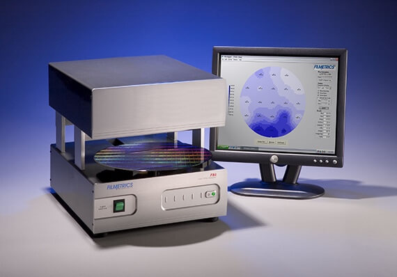
Filmetrics introduces the F60-t tabletop and F60-c cassette-to-cassette instruments for blanket wafer film measurement on up to 300mm diameter wafers.
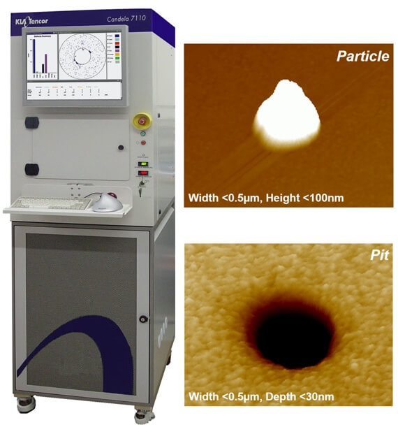
The Candela 7100 and 7120 series systems include the unique capability to discriminate submicron pits from particles on HDD metal substrates.
The Candela 7100 and 7120 introduce two new scatter channels to enhance defect detection and classification capability on hard disk drive substrates. The new stealth scatter channel improves capture of submicron-height defects by suppressing background noise. Comparing signals from the new normal scatter, new stealth scatter, and existing oblique scatter channels enables discrimination of submicron pits from particles, an important innovation because particles may be cleanable, while pits are not. In high sensitivity mode, defect sensitivity is enhanced to 40nm on metal substrates.
Learn more about our latest offerings in this product series: Candela® defect inspectors

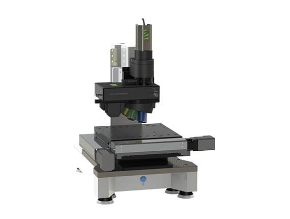
The Zeta™-20 is the first product release from Zeta Instruments.
The Zeta-20 is the industry’s first optical profilometer to use ZDot™, a patented technique that combines structured illumination, confocal optics to generate high resolution 3D surface topography data and a True Color image of the surface. This technique enables users to easily focus on any transparent or opaque surface, for fast measurements of step heights and roughness. Multi-Mode optics expand the capability of the non-contact 3D surface profiler by combining ZDot with white light interferometry, shearing interferometry, a reflectometer for transparent thin-films, and automated defect inspection.
Learn more about our latest offerings in this product series: Zeta-20
The Zeta-200 releases with an automated X-Y stage and new functionality that supports LED applications.
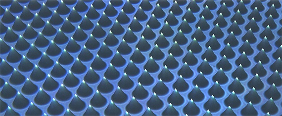
The Zeta-200 optical profiler takes advantage of a high-transmission optics design, backside illumination and proprietary algorithms to measure Patterned Sapphire Substrates (PSS). The system can accommodate a variety of PSS bump shapes, measuring the height and pitch of all PSS bumps in the field of view, thus avoiding false bump signatures or results skewed by measuring only a small area. With Multi-Mode optics, the system is also able to measure thin film thickness and sample bow during PSS manufacturing. Finally, with automated defect inspection, the Zeta-200 can identify defects such as missing bumps, scratches, and particles.
Learn more about our latest offerings in this product series:
KLA-Tencor releases the Alpha-Step D-100 and D-120 based on the Ambios Technology platform, featuring enhanced optical lever sensor technology with significant improvement in measurement stability.
Simultaneous normal-incidence reflectance and transmittance measurement capability is introduced with the Filmetrics F10-VC, which can also be used to accurately measure absorption.
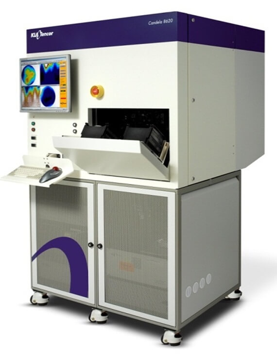
The Candela 8600 and 8620 series release with integration of a new photoluminescence channel for capturing GaN defects that are not visible to typical scatter channels.
The Candela 8620 series are designed for substrate wafer quality inspection and gallium nitride (GaN) epi process control in the LED industry. This new inspection platform integrates proven Candela inspection techniques with a new photoluminescence mode to capture both surface defects and multiple quantum well (MQW) defects. In addition, the 8600 series systems provide the unique capability to detect cracks and differentiate submicron pits from particles on LED wafers.
Learn more about our latest offerings in this product series:
Nanomechanics, Inc. launches the industry’s first high temperature in-situ nanoindenter, the InSEM HT system, with a maximum temperature of 300°C.
The Filmetrics F10-RTA reflectance/transmittance/angled reflectance instrument adds an additional optical subsystem to the F10-VC to measure reflectance at an angle. Results can be combined with the normal incidence reflectance and transmittance data to measure n and k of a thin film without requiring an n and k model.
The Filmetrics F50-XY-510 motorized thin-film mapping instrument features an X-Y translation system for measuring samples up to 510mm by 510mm.
Using a color-coding optical design, the new Filmetrics F70 can measure films from 50µm to 15mm thick.
The Zeta-280 adds a single cassette, benchtop handler to the Zeta-200 platform.
The new Zeta-300 profilometer supports measurement of devices with larger X-Y and Z dimensions. The system is isolated from environmental noise with an integrated isolation table and an acoustic isolation enclosure.
Microfluidic device support is released on the Zeta-20 utilizing ZDot and the transparent, multi-surface measurement application.
The Zeta-20 uses ZDot technology and the multi-surface application to provide an innovative measurement solution for encapsulated microfluidic devices. The high-transmission optics design allows the ZDot signal to remain strong even after passing through multiple layers. This enables measurement of the thickness of the cover plate, channel depth, and the dimensions of the control structures within the microfluidic channel before and after encapsulating the device with cover glass. Measuring after encapsulation is critical since encapsulation can change the channel and control structure shape, impacting the performance of the device.
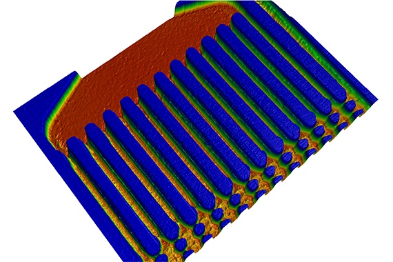
The Zeta-380 combines the benchtop handler from the Zeta-280 with the Zeta-300 platform.
The new Filmetrics aRTie instrument simultaneously measures reflectance and transmittance spectra, includes a 40,000-hour light source, and is powered through the USB interface cable.
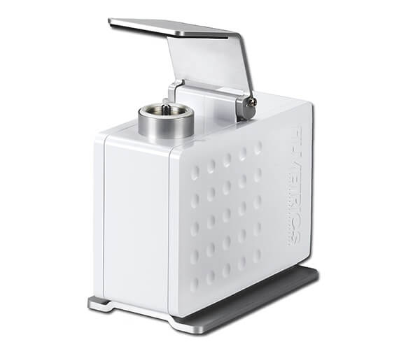
Filmetrics F10-ARc – compact, portable instrument for plastic lens coatings.
The Filmetrics F10-ARc is built for measuring coatings on ophthalmic lenses. The instrument quickly and accurately measures antireflection coatings and hardcoat coatings on plastic lenses used in eyeglasses and other eyewear. The patented, low-power light source used in the F10-ARc enables the system to be compact and portable, drawing power through the USB interface cable.
Learn more about our latest offerings in this product series: Filmetrics F10-ARc
Automatic wavelength calibration is now offered on some Filmetrics instruments, using an integrated gas-discharge lamp to facilitate dramatically improved accuracy and stability.
The temperature range of the InSEM HT system is extended to 500°C. Nanomechanics also launches Express Test, a revolutionary high-speed nanoindentation technique that maps mechanical properties and provides statistical sampling of material constituents.
The new Tencor P-7 and P-17 products feature industry-leading measurement precision, the highest resolution color camera available on a stylus platform, and new performance specifications for long-scan capability critical for bow and stress measurements.
Using a motorized R-Theta stage, the Filmetrics F54 microscopic-spot mapping instrument offers automated sample mapping with a measurement spot size as small as 2.5µm.
The Filmetrics SS-XY-38 motorized X-Y-Z sample stage has an X-Y travel of 38mm, optional motorized focus and can be combined with a new or existing instrument, such as the Filmetrics F20.
The Candela 8720 system delivers a 4x improvement in positioning accuracy over its predecessor, the Candela 8620. It features an improved handler module, and enhanced defect detection and classification on III-V (GaN, GaAs, InP) epitaxial films for LED, communications (RF, 5G, VCSEL, Photonics) and other high-end compound semiconductor applications.
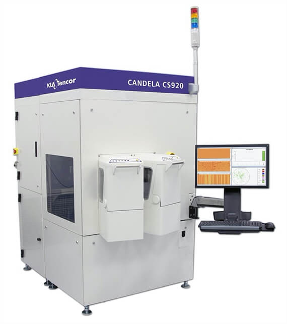
The Candela CS920 releases with a UV laser designed for high sensitivity to defects on Silicon Carbide substrates and epitaxy layers.
The Candela CS920 systems are the power device industry’s first integrated surface and photoluminescence defect detection systems for Silicon Carbide (SiC) wafers. The Candela CS920 platform is equipped with a ultra-violet (UV) laser that enables complete back-side elimination on visually transparent SiC substrates and high sensitivity to nanometer-level scratches on SiC substrates. These scratches can impact epitaxy yield. The new system design enables detection and classification of SiC epitaxy layer surface defects including surface triangles, carrots, and down fall, plus crystal defects including stacking faults and basal plane dislocations (BPD).
Learn more about our latest offerings in this product series:
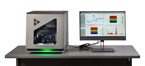
Nanomechanics releases the iNano®, the industry’s most affordable, compact nanoindenter, along with the NanoFlip, a high performance in situ system.
The new iNano is the first affordable, compact and user-installable nanoindenter from Nanomechanics. The iNano introduces improved actuator InForce 50 and controller technology, coupled with a software package focused on ease-of-use. The NanoFlip utilizes the same innovative technology as the iNano in a form factor that enables highly stable in situ measurements.
Keysight Technologies is spun off from Agilent Technologies, taking with it the nanoindenter product line.
The MicroXAM-800 combines the best hardware and algorithms from the Ambios and ADE Phase Shift interferometry platforms with new, innovative, easy-to-use software for automated measurements of step height and roughness.
The Alpha-Step D-500 and D-600 tools release with the same high-resolution camera as the P-7 and P-17 platforms. They are the only stylus profilers to feature keystone correction, to remove distortion from the side-view optics, and they provide improvements in the optical lever, scanning stage, and isolating heat sources that result in better measurement repeatability.
Combining Filmetrics color-coded measurement technology with an R-Theta stage for samples up to 300mm in diameter, the Filmetrics F57 CTM mapping instrument can measure film thicknesses from 50µm to 15mm.
Accurate measurement of the transmittance spectrum of curved samples such as lenses can be accomplished with the Filmetrics SS-Trans-Curved Stage.
Providing improved reliability, digital and USB-based control of all functions and lamp-life meters, the Filmetrics LS-DT2 UV-Vis-NIR fiberoptic light source is designed to pair with Filmetrics instruments that include UV spectrometers.
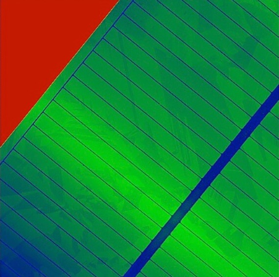
The Zeta-20 releases with enhanced performance that addresses the unique challenges of the solar industry.
The Zeta-20 provides innovative solutions for the solar industry to measure 3D surface topography of the texture process and metal contact lines. Texture measurements are critical to control the pyramid structures’ height, shape, and size distribution, impacting the light capture efficiency of the solar cell. The silver contact lines are deposited with a silk screen process, resulting in large variations in the width, height, volume and electrical resistance of the contact line, as well as the cost of the device. The High Dynamic Range (HDR) measurement mode was developed to address materials with very different reflectivities. For solar cell manufacturing, HDR mode is required to measure the silver contact lines deposited on the pyramid texture with an antireflective coating.
Learn more about our latest offerings in this product series:
The Zeta-360 and first-generation Zeta-388 products provide new options for automated wafer handling capability on the Zeta platform.
Nanomechanics, Inc. releases the iMicro nanoindenter, providing extended force range with the new InForce 1000 actuator. Nanomechanics also introduces NanoBlitz 3D technology, high-speed nanoindentation for mapping mechanical properties.
Utilizing a motorized turret, wafer-handling robot, optional pre-aligner, and a precision optical alignment mechanism, the Filmetrics F64-c cassette-to-cassette tool uses a spot size as small as 1µm to measure thin films on patterned wafers.
The Filmetrics -sX family of instruments, such as the F3-sX, can measure films up to 3mm thick and Si wafer thicknesses up to 1.3mm.
The Filmetrics XY10 motorized stage can be added to most Filmetrics instruments to perform mapping of film thickness or refractive index with measurements as fast as 0.2s per point. The XY10 can include optional motorized autofocus.
Nanomechanics extends the NanoBlitz 3D technique by adding Continuous Stiffness Measurement (CSM) capability. Used together, these technologies can measure mechanical properties as a function of volume, i.e. mechanical property tomography. The InSEM HT temperature range is extended to 800°C.
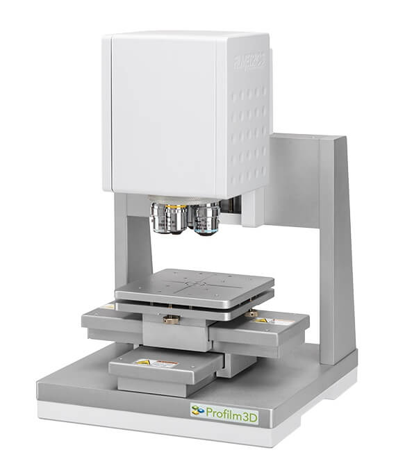
The Profilm3D optical profiler is launched, providing an affordable interferometry-based 3D surface topography measurement solution.
Incorporating design optimizations from its successful thin film reflectometer product line, Filmetrics develops an affordable, easy-to-use optical profiler with multiple imaging techniques to address a wide variety of applications, including film thickness, surface roughness, step height, and topography.
Learn more about our latest offerings in this product series:
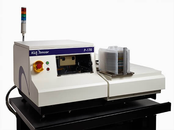
The Tencor P-170 combines the performance of the P-17 with the production proven performance of the HRP handler, enabling fully automated measurement capability for the compound semiconductor market.
The P-170 and HRP-260 tools launch with enhanced, production-proven measurement stability and tool matching. The new platforms feature significant improvements in pattern recognition with the addition of geometric pattern recognition, improved accuracy in the deskew algorithm, and new methods for automatic light control. The handler includes new electronics and support for transparent samples such as silicon carbide (SiC) and sapphire, and for opaque samples such as silicon, gallium arsenide (GaAs) and AlTiC. These innovations enable industry-leading, fully automated surface topography measurements with advanced pattern recognition, matching, automated data analysis capability and support for the latest SECS/GEM automation standards.
Learn more about our latest offerings in this product series:
Nanomechanics releases the Gemini 2-axis isometric indentation system for tribology, wear, and single-asperity testing. Gemini is the only actuator that senses and applies force along both axes, with equivalent resolutions, allowing true nano-tribology and the ability to measure Poisson’s ratio.
Zeta Instruments joins the KLA Instruments group, expanding KLA’s optical profilometer product line, adding ZDot and Multi-Mode measurement technology. The Zeta series support R&D, production, and fully automated cassette-to-cassette environments for the measurement of 3D surface topography.
Zeta Instruments joins the KLA Instruments group, expanding KLA’s unpatterned wafer inspection product line, adding line scan technology on the ZetaScan platform. The ZetaScan supports R&D and production environments for detection and classification of defects on square or round GaAs, glass and sapphire wafers for solar, PV and display applications
The Candela 8420 systems feature hardware and software design improvements that boost throughput by up to 70% over the CS20. The 8420 series supports process monitoring, tool monitoring and tool qualification.
KLA-Tencor Corporation acquires the nanoindenter product group at Keysight Technologies and Nanomechanics, Inc.
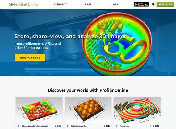
The Filmetrics ProfilmOnline® software enables users to store, share, and analyze 3D data without the need for a desktop computer.
Leveraging the capabilities of web browsers and powerful smart phones, Filmetrics launches the world’s only web application dedicated to the online storing, viewing, and analyzing of 3D topographical data, like those acquired by optical profilers, scanning probe microscopes (such as AFMs), and other 3D imaging microscopes. Users can seamlessly upload data from their Filmetrics Profilm3D optical profilometer with a single click, analyze them, and share the image and measurement results with colleagues. Dedicated phone and tablet applications allow users to view their data on any device, from any location.
Learn more about ProfilmOnline: ProfilmOnline
The Zeta-388 wins the 2018 Compound Semiconductor industry metrology award for patterned sapphire substrate (PSS) applications.
TotalFocus® capability is added to the Profilm3D, providing 3D natural color images of their sample surface with every pixel in focus.
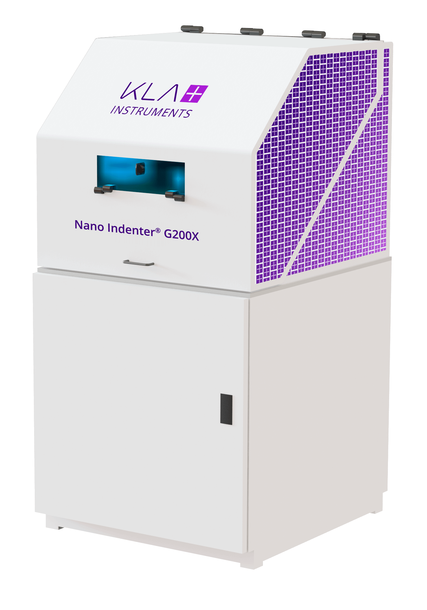
The Nano Indenter® G200X is released by KLA, based on the Nano Indenter G200 and featuring significant improvements to performance and ease-of-use.
The Nano Indenter G200X is faster than its predecessor, the G200, with higher performance and accuracy. New features include DataBurst impact hardness testing, with a 100kHz data acquisition rate, enabling hardness measurements at strain rates exceeding 104/s.
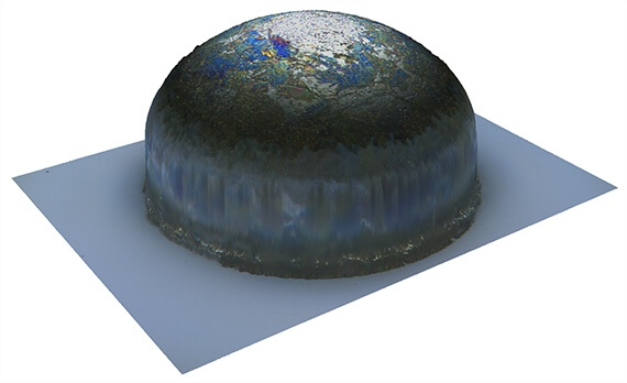
The Zeta-388 is the latest generation optical profiler with cassette-to-cassette wafer handling capability.
With the addition of automated wafer handling capability, new data analysis software, and support for SECS/GEM, the Zeta-388 is designed for fully automated measurements within a production fab. Fast, high-resolution measurement of shallow steps is now possible with the addition of phase shifting interferometry and new automated multi-cursor data analysis. Fully automated measurement of deep, high aspect ratio trenches is enhanced with new light sources. The system provides production-worthy process control measurements, such as bump height on patterned sapphire substrates, roughness, and step height.
Learn more about our latest offerings in this product series: Zeta-388
Filmetrics Joins KLA.
Filmetrics joins the KLA Instruments group on March 6, 2019 and becomes Filmetrics, A KLA Company. The Filmetrics series of thin-film measurement instruments expands KLA’s benchtop metrology capabilities into measurement of film thickness, n, and k. The Filmetrics Profilm3D optical profiler extends the line of KLA instruments that measure surface topography, providing a new option for applications that don’t require the full capabilities of KLA’s existing instruments. Filmetrics worldwide application support and sales offices continue to provide rapid response to customer needs.

Learn more about Filmetrics: Filmetrics
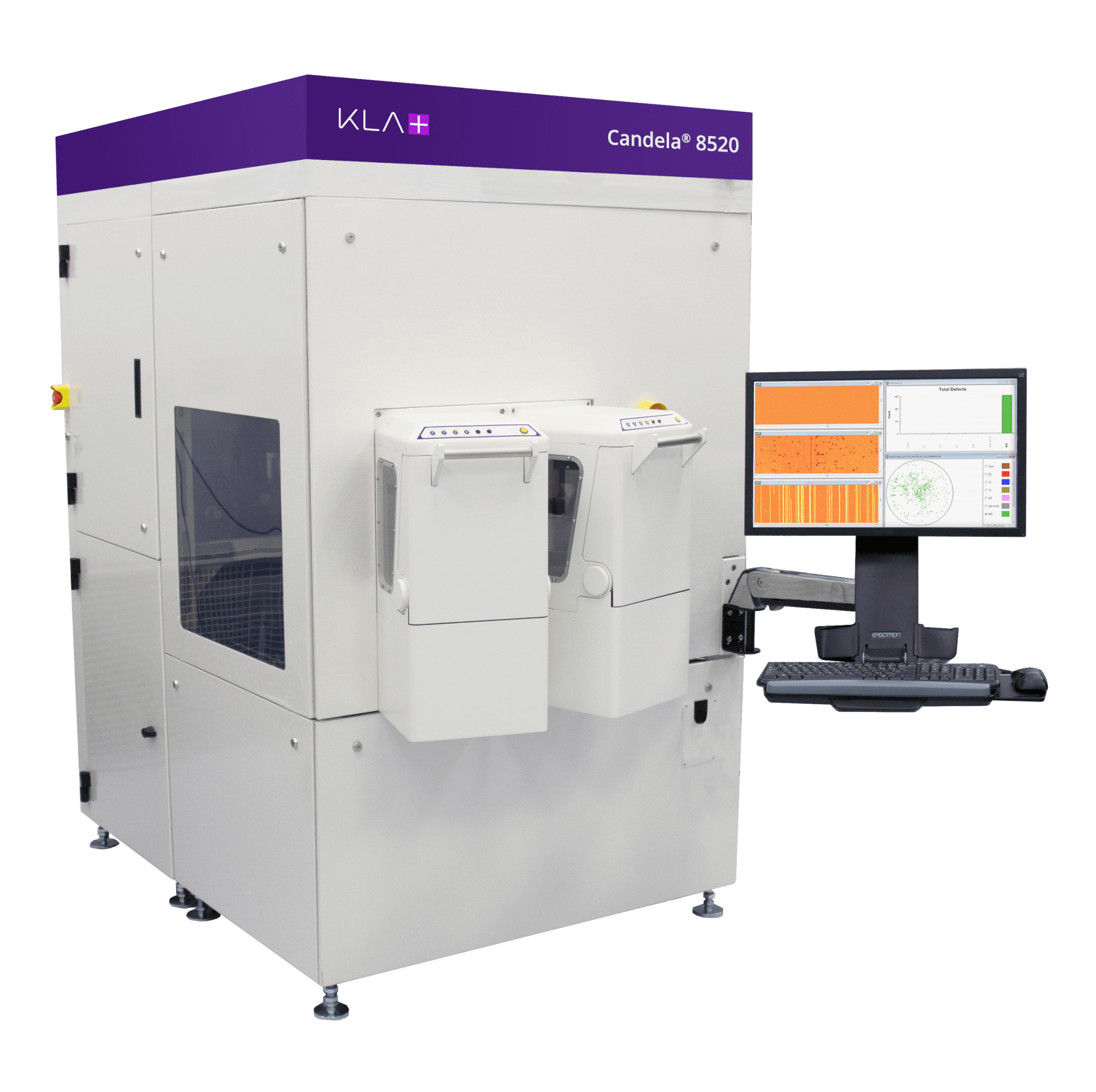
The Candela 8520 system retains the innovative technology of the Candela CS920 while boosting throughput by up to 2.3X. The 8520 also introduces the capability to detect stacking faults on SiC substrates and delivers improved detection and classification of basal plane dislocations on SiC epitaxial wafers.
Learn more about our latest offerings in this product series:

The Profilm3D-200 features a motorized stage with 200mm travel and an adapter for 200mm diameter wafers.
Building on Filmetrics thin-film metrology expertise, Filmetrics introduces the F54-XY-200, an enclosed film thickness mapping system. Using easy-to-create pattern recognition recipes, the F54-XY-200 measures samples up to 200mm using a motorized X-Y stage that moves automatically to specified measurement locations, facilitating thickness measurements as quickly as two points per second. The multi-objective turret offers flexible field-of-view and spot size configurations for a wide range of sample feature sizes.
KLA Instruments introduces the Filmetrics® Gen 5 Profilm3D®, a high-performance incarnation of the successful Profilm3D optical profiler. New imaging modes enable the Profilm3D optical profiler to measure an even wider range of surfaces, including higher surface roughness and steeper slopes.
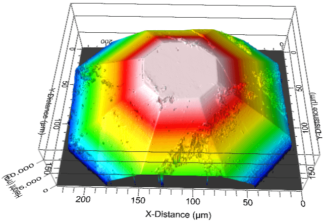
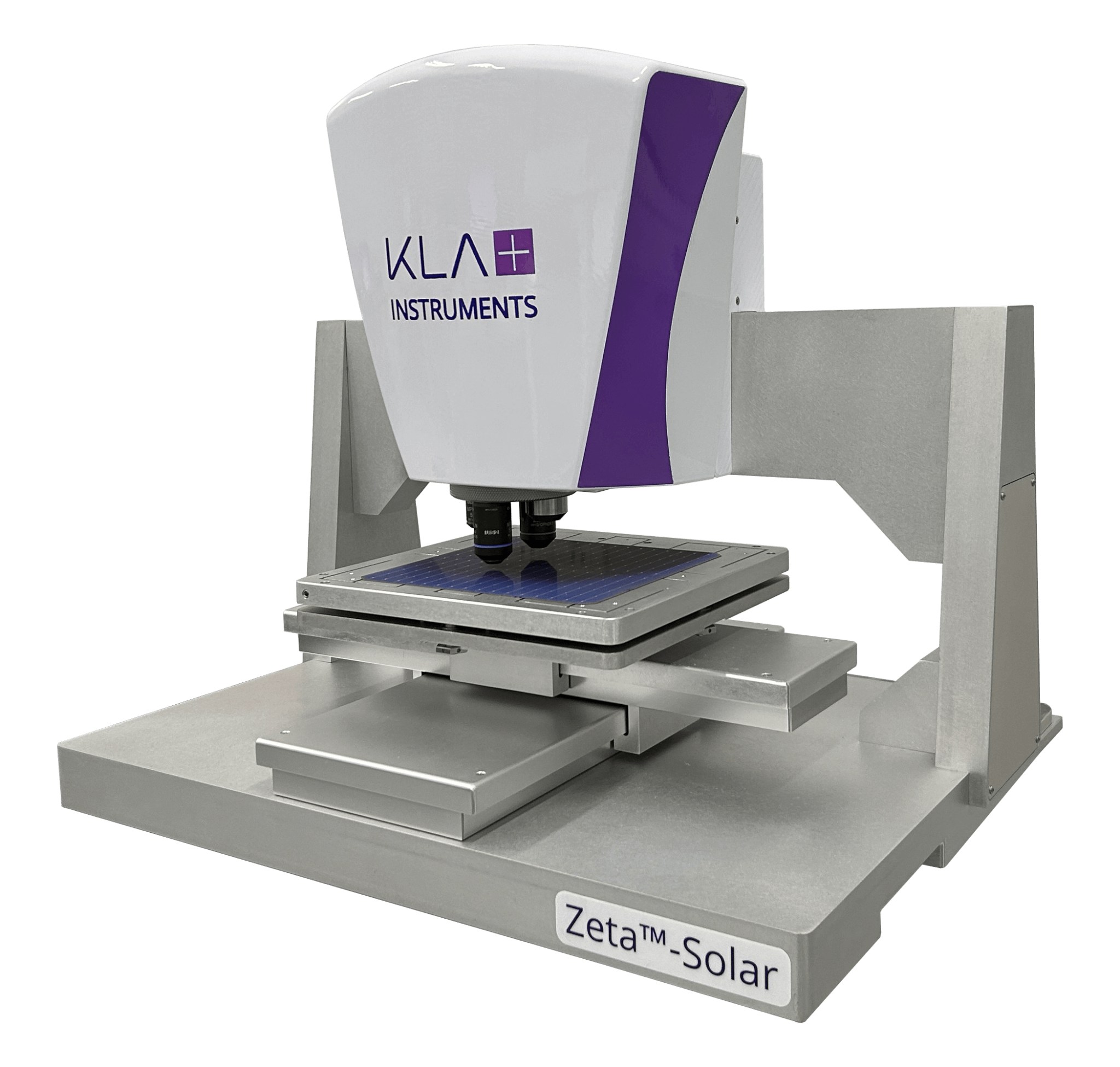
KLA Instruments™ introduces the Zeta-Solar optical profiler, specifically designed for advanced metallization finger, bond/contact pad and busbar solar process metrology, as well as next generation R&D development. This new Zeta model leverages advances in 3D imaging technology to deliver the ideal purpose-built metrology tool for end-of-the-line solar process development and process quality control.
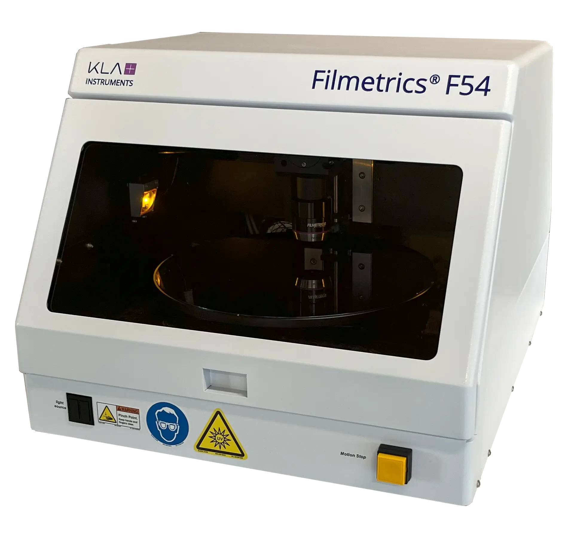
Filmetrics adds the F54-XYT-300 to the successful F54-XY series of enclosed, automated film thickness mappers. Measurements of 300mm wafers are supported by the additional high performance rotary stage in the F54-XYT-300 configuration and expanded pattern recognition functionality to support small-spot thickness measurement. The IR Camera option was also introduced for imaging through thinned silicon, a feature that appeals to quantum computing F40 users for targeted gap measurement. Both the 200mm and 300mm systems support measurement of either unpatterned samples or patterned samples using pattern recognition software.
Learn more about our offerings in this product series: